
Building the IBM Spyre Accelerator
Release
Peter Hess
IBM Research scientists are using AI to track down defects and inefficiencies in silicon wafer processing.
The silicon wafers that form the basis for modern chips are extremely sensitive. As they’re being manufactured, there are many steps where defects can be introduced. To smooth out this process and ensure that defective chips are caught as early as possible, IBM Research scientists are proposing new algorithms to identify the source of defects across a whole range of chip making processes, and challenging a longstanding assumption about controlling silicon wafer workflow.
A team led by Tsuyoshi Ide, head of data science for semiconductors at IBM Research, is presenting three papers on this work at the Advanced Semiconductor Manufacturing Conference (ASMC) taking place May 5 to 8 in Albany, New York. The AI algorithms that Ide and his team are developing rely on IBM’s SiView and Intelligent Fab data platforms for semiconductor manufacturing.
Wafer manufacturing includes a dozen different process types such as etching and deposition, more than half of which must be repeated 40 to 100 times per layer, meaning there’s potentially 1,000 or more steps involved in making a chip — each one bringing the potential for defects. Quality control inspectors use microscopes to quantify how good or bad a silicon wafer’s quality is, according to how dense the defects are.
If something goes wrong, though, tracking down the culpable tooling machine or exact source of the error can be extremely difficult. The result of each step depends on the fidelity of all the steps that came before it, so multivariate errors can add up without a single clear source.
Ide likens the history of a silicon wafer to a human life: “One very small screw-up in the early stage of your life may significantly affect your life trajectory,” he said. Similarly, a manufacturing imperfection at some stage of wafer production can create untold effects down the line. “Because of the sequential nature, analyzing root causes is very, very challenging,” Ide added.
There’s no solution available, as this isn’t a standard machine learning problem. “Machine learning is good at predicting something when given a complicated set of inputs, but this is kind of an inverse problem,” said Ide. Rather than predicting a next step or end result given a series of inputs, the IBM Research team is trying to retroactively identify a single step based on the final output. Practically speaking, the only way to do this would be to fabricate wafers over and over and over, with varying conditions, then apply simple statistical analysis to figure out where defects are occurring — in other words, the scientific method. This is totally impractical for all but the biggest chip manufacturers, but even then, this semi-manual approach requires a massive team of researchers and managers, so it pushes against the limits of practicality.
As an alternative to running wafer after wafer after wafer, Ide and his team are trying something else.
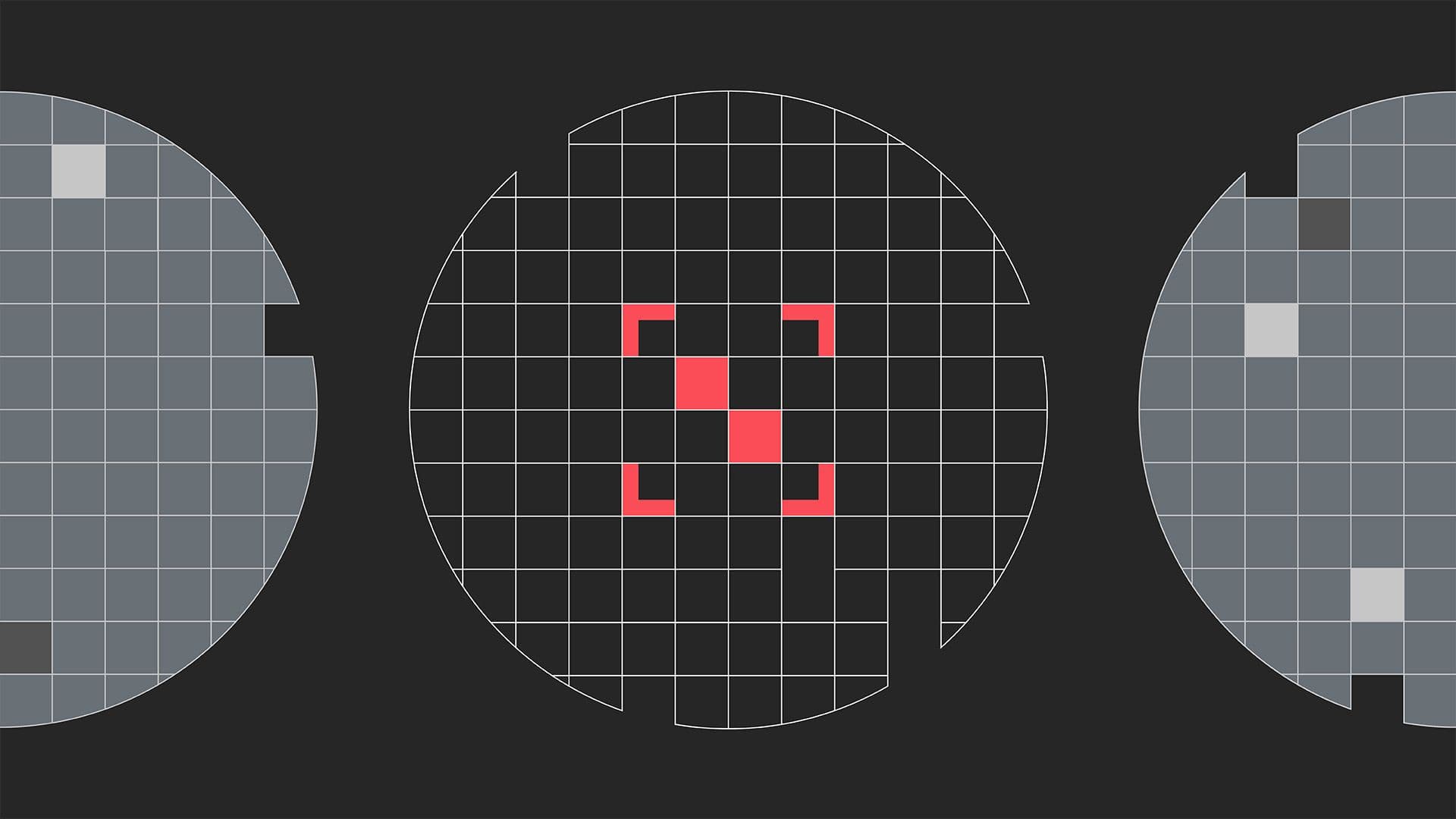
In their first paper, the team sought to identify which measurements along the way are most relevant to the occurrence of a certain type of defect. To do that, they computed the attribution score for each parameter measured. Each of the processing tools handles very different physical processes — doping, polishing out roughness, grinding away material, and so on — so it’s hard to compare data among different parts of the wafer production process. Instead they use a so-called inline measurement, typically made right after a major process is completed.
These inline measurements can be proxies of each step’s fidelity, and based on them, the team trained a classifier to compute a responsibility score for each item.
In this figure, there’s one point in the processing timeline that the model predicted a big jump in the probability of a bad wafer — a ‘badness’ prediction, in short. That analysis means two things. The first is that timestamp is relevant to that defect in some way, and the second is that the wafer was predicted to be bad months before the final measurement. “So you could stop the process if you knew this fact,” said Ide.
Their scoring algorithm, called the Trajectory Shapley Value, a novel extension of the well-known Shapley value algorithm in game theory, is meant to give engineers some priority recommendations. With this particular model, Ide and his colleagues don’t try to guess what exactly is going on with the machines, they just identify the time when something goes wrong.
In a second paper, they used a different type of model. Instead of a good-bad classification, this trajectory-based prediction model predicts actual defect density and tries to identify which process is most responsible.
Again, responsibility scores are calculated, but this time they come from process attributes — wafer quality data collected throughout the manufacturing process. But how do you convert process attributes into numbers that you can analyze? For this they propose a technology called proc2vec, an approach inspired by word2vec, a well-known technique in natural language processing. Much like a transformer automatically analyzes the interdependency between words without being given explicit grammar knowledge, proc2vec is meant to automatically capture hidden dependencies among silicon wafer processes and inline measurements.
For example, using wafer history data from IBM Research Albany, the team demonstrated that incorporating these interdependencies significantly enhances defect prediction accuracy. Their new attribution method, built on the trajectory-based model, successfully identified potentially anomalous processes caused by unusually long waiting times.
The team’s third paper takes aim at WIP (work in-progress) bubbles in the fab, which is rather like traffic congestion of wafer lots, or groups of wafers going through the build process at the same time. Wafer lots move around a fab’s railway at different rates, so there can be a surprising amount of randomness.
To understand how wafer traffic gets jammed up, fabs use an advanced semiconductor manufacturing simulator (ASMS), like a traffic simulator for city planning. Running the ASMS is computationally demanding, so a simplified model has been used for many years, called queuing theory. Queuing theory may use assumptions that are too simple, though, which can underestimate how truly variable a fab can be, according to Ide.
Using an alternative mathematical model called the Hawkes process, which accounts for event history, the team analyzed data from IBM Research Albany’s wafer history. They found this approach, evaluated using a statistical model selection criterion called the Akaike Information Criterion (AIC), provides a much better fit between predicted lot arrival times and the actual times compared to queuing theory assumptions.
A measure they used is called ‘X-factor,’ the ratio between actual cycle time and ideal cycle time, which would be the shortest processing time assuming only one wafer exists in the entire fab — no waiting time, just moving and tooling. “So typically X-factor is much more than 1, typically 10 or 15,” said Ide.
They found that non-uniformity in lot arrival times at certain tool positions dramatically increased the time it took to complete the wafer. Following their model, it turns out that if average tool utilization is controlled, X-factor can be much bigger than the traditional queuing-based model would predict.
This suggests traditional queuing theory-based WIP analysis need to be revised, at least for semiconductor manufacturing. This paper points out the problem with the existing approach, but it doesn’t necessarily propose a solution. It does, however, suggest that the Hawkes model is better.
Much of this work is in its early stages. Along the way, the team identified a major limitation: that we only have superficial information about process parameters. To address that, the IBM Research team plans to incorporate physics-based information in their future work.
Long term, their goal to apply these learnings and models to real production lines to improve the quality of wafer fabrication runs in the future.